
www.industry-asia-pacific.com
21
'26
Written on Modified on
Semiconductor Materials Manufacturing for Sub-2nm Process Nodes
BASF and Taiwan Ministry of Economic Affairs expand chemical production infrastructure to resolve sub-2 nanometer material purity constraints.
www.basf.com
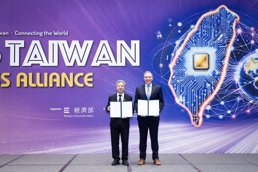
BASF signed a Letter of Intent with Taiwan’s Ministry of Economic Affairs to expand manufacturing capacity, analytical capabilities, and laboratory infrastructure for advanced semiconductor materials. The joint initiative targets critical fabrication parameters for process nodes below 2 nanometers in the high-performance computing, artificial intelligence hardware, and microelectronics sectors.
Operational Challenges in Sub-2nm Node Fabrication
Scaling integrated circuit architectures below 2 nanometers introduces severe process sensitivities during lithography, etching, and planarization. Defect density thresholds tighten significantly at these geometries, making sub-microscopic particulates and chemical impurities critical points of failure. Addressing these constraints requires specialized chemical formulations engineered to maintain stability at molecular tolerances, alongside local supply lines that prevent chemical degradation during transit.
Technical Infrastructure and Site Expansion
Under the framework of the agreement, BASF expands its existing facility in Kuanyin, Taoyuan. The project incorporates new production units configured for ultra-high-purity chemical processing, accompanied by an expanded Innovation Center with specialized quality analysis instrumentation. BASF manages the formulation engineering, quality control metrology, and scaled manufacturing of wet chemicals and specialty materials. The Ministry of Economic Affairs facilitates industrial integration and coordination within the broader regional semiconductor manufacturing ecosystem.
Process Integration and Analytical Metrology
The facility expansion supports leading-edge fabrication workflows, including chemical integration with extreme ultraviolet photolithography, precision deposition, and post-etch surface cleaning. The analytical laboratory provides automated impurity profiling to detect metallic and organic contaminants down to parts-per-trillion levels. This testing infrastructure provides immediate feedback loops between chemical synthesis and wafer processing requirements, aligning output with baseline international microelectronics cleanliness standards.
Supply Chain Stabilization and Scalability
Locating chemical synthesis and analytical testing in geographic proximity to major wafer fabrication facilities reduces supply chain vulnerabilities and transport lead times. In addition to securing continuous material supply for high-volume fabrication lines, the integrated analytical center accelerates qualification cycles for next-generation material variants.
Regarding the engineering and logistical objectives, Jens Liebermann, Senior Vice President of the Global Electronic Materials business and Chairman of BASF Taiwan, stated: "By strengthening our local manufacturing, innovation, and technical service capabilities, we are deepening collaboration with our customers and accelerating the development of materials solutions for future technology generations, while further enhancing supply chain resilience."
Edited by Natania Lyngdoh, Induportals editor, with AI assistance.
www.basf.com
