
www.industry-asia-pacific.com
16
'26
Written on Modified on
Automated Inspection for High-Density Semiconductor Substrates
Nidec Advance Technology showcases optical, electrical, and X-ray inspection equipment at TPCA Show TAIPEI 2026 to verify heterogeneous integration packaging.
www.nidec.com
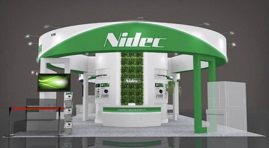
TPCA Show TAIPEI 2026 takes place from Tuesday, October 20 to Thursday, October 22, 2026, at the Taipei Nangang Exhibition Center in Taipei, Taiwan, highlighting manufacturing and test innovations across the printed circuit board and electronic packaging industries. At Booth K-725, Nidec Advance Technology Corporation presents inspection and material handling systems engineered for high-density substrates, fan-out panel-level packaging, and advanced semiconductor carrier architectures.
Core Technology and System Architecture
The exhibition lineup covers electrical conduction, insulation testing, and non-destructive optical metrology configured to verify fine-pitch interconnects. For electrical continuity, the GATS-7885 executes open and short-circuit testing across fan-out panel-level packaging and redistribution layers, while the GATS-8360 accommodates chip-on-wafer-on-package large high-density interconnect substrates. Optical analysis is managed by the RSH series for two- and three-dimensional surface verification and the AURCA series, which employs machine learning algorithms for defect classification on optical modules and wide-area panels. In subsurface defect analysis, a high-speed computed tomography X-ray system evaluates depth and alignment parameters in PCB back-drilling processes.
Deployment or Implementation
Testing units integrate within front-end semiconductor packaging environments and high-volume printed circuit assembly lines. The AVR SMV 3000 equipment front end module, developed jointly with Nidec Instruments Corporation, provides automated substrate and wafer loading directly to inspection stages. Narrow-pitch NS probe fixtures interface with STAR REC V6 testers to maintain electrical contact stability on high-pin-count substrates, while specialized optical sensors verify through-glass via structures during panel processing.
Industry Applications
The inspection portfolio serves advanced semiconductor packaging facilities, high-density interconnect fabricators, and communication hardware manufacturers producing artificial intelligence accelerators and high-performance computing modules. As multi-die packaging shifts toward larger package dimensions and tighter line spacing, physical warpage and micro-shorts create severe yield risks. Standardizing continuous optical, electrical, and radiographic screening across bare substrates eliminates defective layers before high-value component bonding stages.
Operational Impact and Performance Metrics
Automated handling via equipment front end modules combined with high-throughput electrical testing minimizes contact damage and cycle times on delicate large-format panels. Computed tomography inspection for back-drilling provides deterministic structural feedback to drilling spindles, reducing via-stub lengths and signal reflections without destructive physical cross-sectioning. Deploying coordinated testing routines across panel production stabilizes manufacturing yields, enhances fault coverage on heterogeneous packaging, and lowers scrap volume across advanced fabrication lines.
Edited by Romila DSilva, Induportals Editor, with AI assistance.
www.nidec.com
