
www.industry-asia-pacific.com
01
'26
Written on Modified on
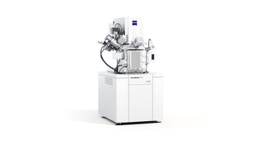
ZEISS enhances FIB-SEM precision with Crossbeam 750
New system combines real-time SEM imaging and FIB milling with Gemini 4 optics to improve endpoint accuracy and 3D analysis workflows.
www.zeiss.com
Semiconductor analysis, materials science, and nanofabrication workflows require precise sample preparation, high-resolution imaging, and accurate endpoint detection at nanometer scale. In this context, ZEISS has introduced the Crossbeam 750 FIB-SEM, designed to enable simultaneous focused ion beam (FIB) milling and scanning electron microscopy (SEM) imaging for continuous process control during sample preparation.
The system integrates real-time imaging with milling operations, allowing users to monitor material removal and structural evolution without interrupting the process. This approach addresses a key limitation in conventional FIB-SEM workflows, where intermittent imaging can lead to inaccuracies in endpoint detection and increased rework.
Real-time “see while you mill” process control
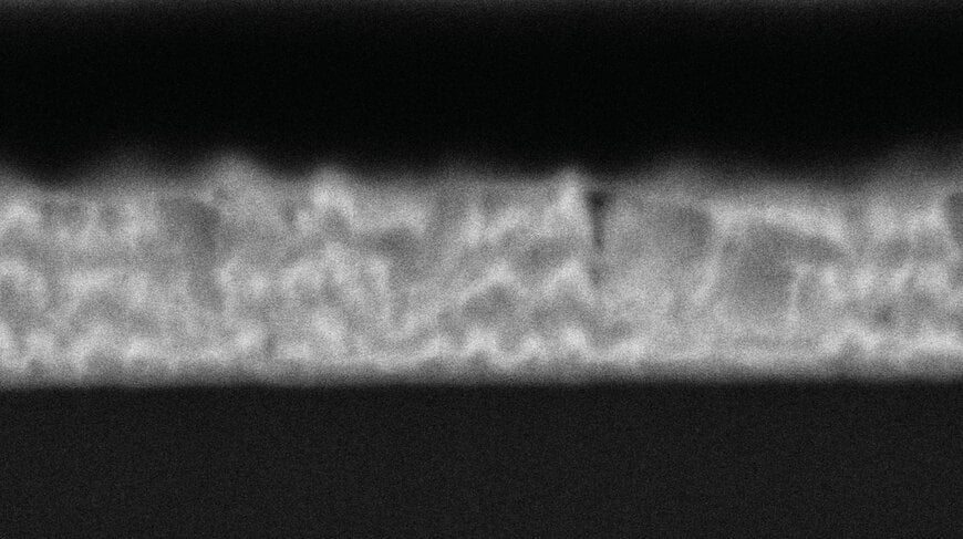
The Crossbeam 750 enables continuous SEM imaging under all milling conditions, from high-current material removal to fine polishing at low accelerating voltages down to 0.5 kV. This capability allows operators to observe FIB–sample interactions directly and adjust parameters in real time.
Such control is particularly relevant in transmission electron microscopy (TEM) lamella preparation, where uniform thickness and minimal damage are required. By maintaining visibility throughout the process, the system supports first-pass success in lamella fabrication and reduces the need for iterative corrections.
Gemini 4 optics for high-resolution imaging
The system incorporates the new Gemini 4 electron optics, which provide improved resolution and signal-to-noise ratio. This enables background-free imaging and stable performance at low landing energies, which is critical for sensitive materials and high-precision analysis.
Enhanced imaging performance supports applications requiring detailed structural characterisation, including advanced semiconductor devices and nanoscale material systems.
Applications in advanced semiconductor and materials workflows
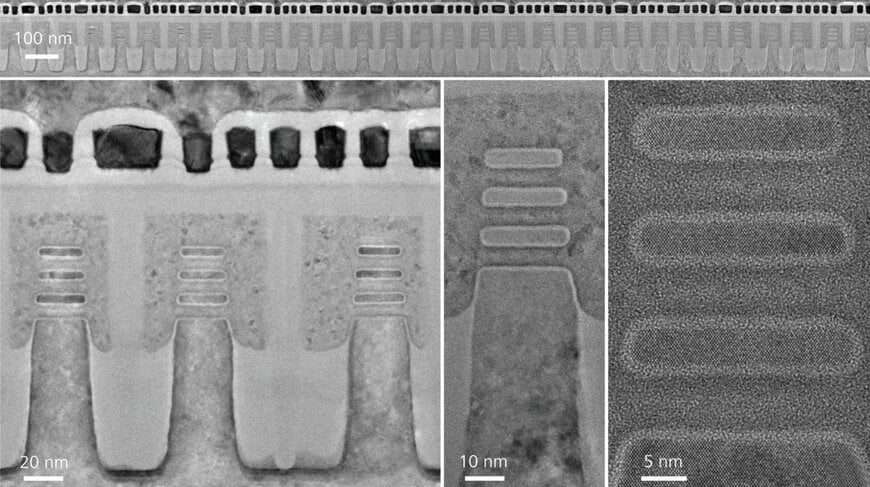
The Crossbeam 750 is designed for use in leading-node semiconductor applications, including logic and memory devices based on architectures such as gate-all-around (GAA) and complementary FET (CFET). These structures require nanometer-scale accuracy during cross-sectioning and sample thinning.
Beyond semiconductors, the system supports a range of materials science and life science applications, including:
- TEM lamella preparation for high-resolution microscopy
- Atom probe tomography (APT) sample preparation
- Nanofabrication processes such as electron-beam lithography
- Three-dimensional (3D) volume imaging and tomography
The system’s large, undistorted field of view improves data quality in 3D tomography, while stable low-kV imaging conditions enhance contrast and reduce acquisition time.
Improved throughput and reproducibility
By eliminating the need to pause milling for imaging, the Crossbeam 750 streamlines workflows and reduces total processing time. Continuous monitoring enables more consistent results, particularly in high-throughput environments where reproducibility is critical.
The ability to achieve precise endpoints on the first attempt is especially valuable in semiconductor failure analysis and process development, where deviations at the nanometer scale can affect device performance.
Positioning within FIB-SEM systems
FIB-SEM platforms are widely used for nanoscale sample preparation and analysis. Comparable systems include Thermo Fisher Scientific Helios series and Tescan FERA platforms, which also combine ion beam milling with electron imaging.
Key differentiators in this segment include imaging resolution at low voltages, real-time process visibility, and field-of-view quality for 3D reconstruction. The Crossbeam 750’s integration of continuous SEM imaging during milling and enhanced electron optics targets these performance parameters, particularly for advanced semiconductor nodes and high-precision materials research.
By combining simultaneous imaging and milling with improved optical performance, the Crossbeam 750 addresses evolving requirements in nanoscale fabrication and analysis, where process control and imaging fidelity directly impact results.
Edited by Natania Lyngdoh, Induportals Editor — Adapted by AI.
www.zeiss.com
