
Beyond Silicon – What Will Replace the Wonder Material?
Milton D'Silva talks about the present state of the silicon-based chips industry and the status of non silicon alternatives for semiconductors in future.
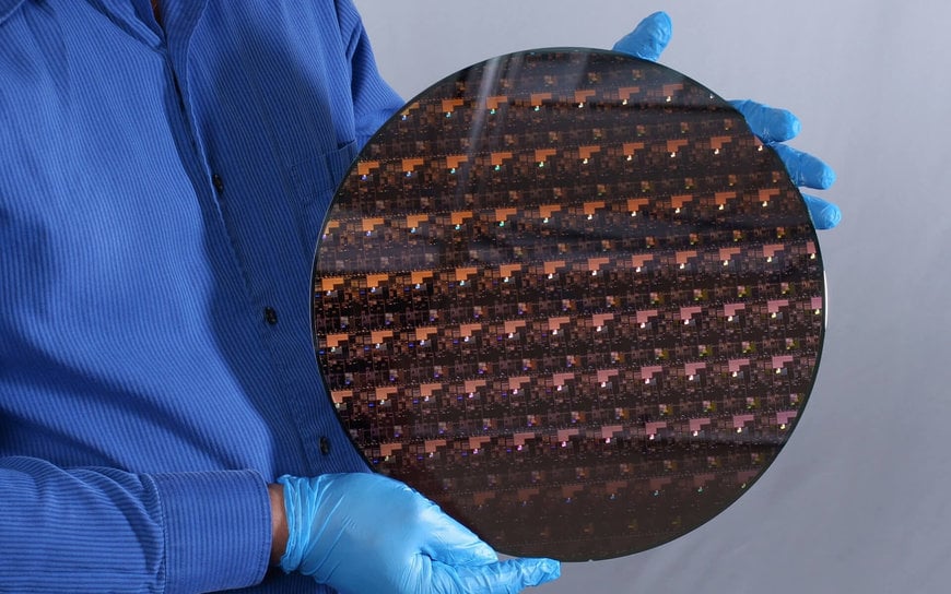
The silicon chip paved the way for the revolution in electronic devices. Image by MasterTux from Pixabay
In late 2004, CNN.com conducted a three-month online survey asking respondents to vote for the most important technology of the past 50 years from a list of 24 inventions. 24% of the 119,000 plus respondents voted for the silicon chip. The fact that the World Wide Web (20%) was placed at number two, the Personal Computer (17%) was third and mobile phone much lower, is indicative of the importance the respondents accorded to the silicon chip that has revolutionised computing in the last 50 years and more.
The chip is an integrated circuit (IC), also called the monolithic integrated circuit or the central processing unit (CPU), which is a flat piece of semiconductor material (mostly silicon, and hence silicon chip) on which are embedded a large number of electronic circuits. The progressive evolution of semiconductor based transistors from the 1950s replaced the vacuum tubes that were bulky and unreliable, and paved the way for the revolution in electronic devices that in turn continues today and is now poised to look beyond silicon.
If one were to go through the history of the evolution of the IC, no single person can be said to have discovered the materials or invented the process that made the early chip. Scores of scientists, engineers and innovators were engaged during that period in finding an effective alternative to the vacuum tubes on which early electronic devices were based. However two persons, who were working independently, are widely credited with the invention of the IC – Jack Kilby (Texas Instruments) and Robert Noyce (Fairchild Semiconductor, later Intel). While Kilby invented the hybrid integrated circuit in 1958, Noyce invented the first monolithic IC in 1959.
The most commonly used IC chips today are based on Noyce's monolithic IC, rather than Kilby's hybrid IC. Noyce, along with his partner at Fairchild Semiconductor, Gordon Moore, founded Intel in 1968 in California, and the company is today the world's largest semiconductor chip manufacturer by revenue. If Noyce was later dubbed as the Mayor of Silicon Valley, Moore is known for the law associated with his name that states the number of transistors in a dense integrated circuit (IC) doubles about every two years, but more of this later. Ironically, by the time the Nobel Prize committee decided to recognise the invention of the IC in 2000 with the Physics Prize, Noyce was dead (1990) and Kilby was the sole recipient, which otherwise would have most certainly been shared by the two. Kilby graciously acknowledged in his acceptance speech the contributions of thousands of engineers and scientists in laboratories and production facilities all over the world in the invention of the IC.

Jack Kilby of Texas Instruments designed the first hybrid integrated circuit in 1958. Source: TI
The rationale for Silicon
Semiconductors are devices with the properties that can switch the current flow on and off at room temperature which is not the case with pure conductors or insulators, and hence the materials of choice for electronic devices. Silicon is not the only material suitable for semiconductors, though it has dominated the electronics industry for decades. In fact silicon is not even the best material for chips on account of its diminishing electrical performance and low thermal conductivity, which necessitates costly cooling systems. Besides, although silicon lets electrons pass through its structure easily, it is not so with the positively charged counterparts of electrons known as ‘holes’. This makes it unsuitable for some types of chips. But transistors can also be made from many other materials, and they are being made, albeit in much smaller numbers. The very first transistor created in 1947 at Bell Labs was made with Germanium, as was Kilby’s hybrid IC, made in 1958. Noyce used silicon in his design which was widely adopted, and hence became the material of choice. On the plus side, it is very easy to create a high quality thin insulator on the surface of a silicon chip by treating it in a furnace with oxygen. All things considered, there is no such thing as a perfect material because the substitute materials too have their own advantages and disadvantages. Perhaps despite some shortcomings, what really tipped the scale in favour of silicon against other materials like Germanium or Gallium, with better electronic properties, is the fact that it is cheap and abundant in nature.
The chip or IC or CPU is the brain of a computer that processes input, stores data and provides the resultant output. The early chip had just a handful of transistors, which are like tiny switches that allow electrical current to pass through a chip that does the actual computing. The Moore's Law referred to in the earlier paragraph is a principle that states the speed and capabilities of computers are expected to double every two years as the number of transistors that fit on a microchip increases. The law holds good even today and presently the number of transistors on a commercial processor is above 100 billion as in the case of Apple's M1 Ultra chip. Nvidia and Intel have similar chips with better capacities in the offing. The debate however is whether Moore's Law will apply in future or is the chip reaching the saturation point and is this the time to look for alternatives – better semiconductors or more research to extend the chip capacity with better design and breakthrough technologies.
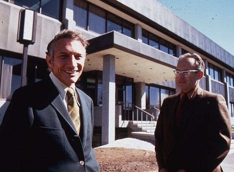
Robert Noyce and Gordon Moore in front of the Intel SC1 building in Santa Clara in 1970. Credit: Intel Free Press
Alternative materials
As seen earlier, the substitutes for silicon were always there even when engineers and inventors were working on the early designs of the ICs. Once the consensus converged on silicon, the tech world having invested billions of dollars and several decades perfecting the process is not in a hurry to give up and start the cycle all over again with a new material. The quest for an IC that is smaller, faster, and cheaper, and above all, one that consumes less power continues, in combination with or independent of silicon. While researchers are working at finding substitutes for silicon or ways to augment it to increase its transistor bearing capacity, several materials like graphene, gallium nitride, black phosphorus and boron nitride nanosheets are under consideration. These are known as 2-D materials, since they are flat sheets only an atom or two thick. But what exactly are the options?
This writer posed the query to ChatGPT, the latest sensation in the tech world that seemingly knows everything, and got an answer in next to no time. There are several alternatives to silicon-based chips, including:
- Gallium Nitride (GaN) chips: GaN has higher electron mobility compared to silicon, allowing for faster switching speed and higher power efficiency.
- Carbon Nanotube (CNT) chips: CNTs have high thermal conductivity and high mechanical strength, making them ideal for high power applications.
- Graphene chips: Graphene has high electron mobility, high thermal conductivity, and high mechanical strength. It is being researched for potential use in electronics, but has not yet been commercialised.
- Organic electronics: Organic electronics are made from carbon-based materials, and are being researched for use in flexible electronics and large-area electronics applications.
These alternatives to silicon-based chips have different properties and challenges, but they hold the potential to improve upon the performance and cost of current silicon-based technologies, informs the AI powered ChatGPT.
GaN or Gallium nitride is a binary III/V direct bandgap semiconductor commonly used in blue light-emitting diodes since the 1990s. GaN transistors are suitable for high frequency, high voltage, high temperature and high efficiency applications, as the material is efficient at transferring current, which means less energy is lost to heat. Though GaN has many serious advantages over silicon as it is more power efficient, faster, and has better recovery characteristics, there are hurdles like the depleted nature of GaN transistors and the inability to produce them at the same scale as current silicon transistors. Companies like Panasonic are pursuing serious research on GaN technology development. In fact Panasonic and Infineon Technologies are jointly working on development and production of the second generation (Gen2) of their proven GaN technology and the market launch of the new 650 V GaN Gen2 devices is planned for the first half of 2023.
Carbon nanotubes (CNTs), which are basically tiny cylindrical sheets of graphene, have better electrical and thermal properties than silicon, but converting them into high-purity tubes to integrate into chips is a major challenge. While it is possible to obtain a purity of 99.99%, the uncertainty of a fraction casts a doubt and will slow or stop the transistor from switching. To withstand this type of failure, advanced circuits will need CNTs at around 99.999999% purity, which is virtually impossible to produce today, and hence not in mass production. But CNTs continue to be used for several other applications and with more research, still hold promise as a possible alternative to silicon chips. To that end, all leading chip companies including TSMC, IBM, Intel and many other research institutes are working on CNT chips along with various universities. A DARPA-led project is also developing 3D devices, which stack memory on carbon nanotube transistors.
Panasonic and Infineon Technologies are jointly working on the second generation of GaN technology. Infineon Press Photo
Among the leading contenders, Graphene is said to be the most promising with its high electron mobility, high thermal conductivity and high mechanical strength. Andre Geim and Konstantin Novoselov were awarded the 2010 Nobel Prize in Physics “for groundbreaking experiments regarding the two-dimensional material graphene”, according to the Nobel Prize committee. The committee also observed that since graphene is practically transparent (up to nearly 98%) whilst being able to conduct electricity, it would be suitable for the production of transparent touch screens, light panels and maybe solar cells. Also plastics could be made into electronic conductors if only 1% of graphene were mixed into them. But experts believe graphene is nowhere close to being a replacement for silicon, as it is still in the development stage and the cost of implementing it into the supply chain would be extensive. In the meanwhile, graphene will be used as an enhancer to improve other devices by extending the lifespan or improving the conduction, as it is presently used to keep mobile batteries cool or add strength to sports gear.
In July 2022, MIT News announced that cubic boron arsenide could be a possible alternative to silicon. Cubic boron arsenide performs better than silicon at conducting heat and electricity. Experiments carried out by a team of researchers at MIT, the University of Houston, and other institutions show that cubic boron arsenide overcomes the two critical limitations of silicon as it provides high mobility to both electrons and holes, and has excellent thermal conductivity. In fact, according to the MIT release, these researchers say cubic boron arsenide is the best semiconductor material ever found, and maybe the best possible one. But as with the other substitute candidates, so far, cubic boron arsenide has only been made and tested in small, lab-scale batches that are not uniform and more work will be needed to determine whether it can be made in a practical, economical form, to even think of replacing silicon.
Yet another 2-D material that could be a good replacement is molybdenum disulfide, which has already been used to create flexible electronics and a simple microprocessor. Once again, it depends on how soon is the world prepared to invest in these materials to make them commercially viable. In the meanwhile, silicon continues to ride high, bolstered by several developments in recent years, more so in the post pandemic era, for reasons that are obvious in the following paragraphs.
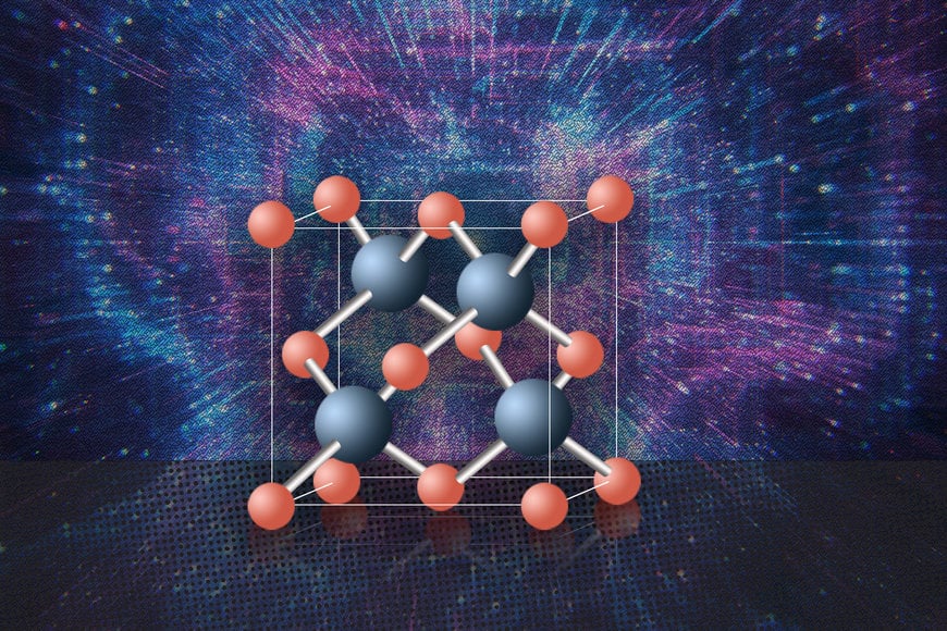
Cubic boron arsenide overcomes the two critical limitations of silicon. Image: Christine Daniloff, MIT
Chips shortage and CHIP Act
As the world had settled comfortably with all the gadgets and gizmos powered by the simple yet complex silicon chip, the pandemic administered a rude shock and not just with the death and devastation it caused. The pandemic by itself did not cause the chip crisis as global manufacturers were already struggling to cope with high demand for them thanks to the growing requirements of Electric Vehicles and the autonomous driving ecosystem. The early phase of the pandemic with stringent lockdown imposed globally however caused a major disruption in production, throwing the supply chains in serious turmoil. The situation was further exacerbated by the rising demand for electronic devices as Work From Home became the norm. The resulting shortage of chips caused widespread havoc in the industry, hitting the automobile sector hard in particular, causing a long waiting list for several popular car models.
The supply chain disruption was also brought home by other incidents like the six days blockage of the Suez Canal in March 2021 caused by the Ever Given, a container ship that had run aground in the canal. The severe storm in the US around the same time disconnecting power lines to a large number of fabs is another example. It was a massive realisation and a huge awakening call for the US industry and the Federal Government that was hit by the sudden realisation of how vulnerable was the US that prided itself on its prowess in the semiconductor industry. As the Intel website acknowledged the obvious, it stated the plain fact that the world desperately needs more geographically resilient supply chains. “Over the past 30 years, the industry went from 80% of semiconductor manufacturing in the west, including the US and Europe, to 80% in Asia. Our moonshot goal is that by the end of this decade, the US will have gone from 12% to 30%; Europe from 9% to 20%; that we’ll collectively go from 20% to 50% by the end of this decade”, it asserts.
The sentiment is shared across the Atlantic, in Europe. “We are all now wiser, and know that the globalisation approach from the old days will not work anymore, full stop! There were challenges and bottlenecks in different countries during Covid, which was normal – problems in cargo shipments, especially in the automotive industry where the Just-in-Time approach would not work anymore. You know what happened with this crisis with microchips. So it is time to rethink the globalisation approach. We should now think of the world as three hubs – the Americas – North and South; Europe; and Asia,” said Michael Ambros, Managing Director, K A Schmersal GmbH & Co KG. As a manufacturer of safety switches including opto-electronic safety equipment, Schmersal's product portfolio includes more than 25,000 products for diverse industries including road and rail transport and aerospace, and the chip shortage hit it hard with the price of a microchip costing USD 1.2, suddenly shooting up to USD 26!
The 2 nm design demonstrates the advanced scaling of semiconductors using IBM's nanosheet technology. Photo: IBM
It is against this background one must view the Creating Helpful Incentives to Produce Semiconductors and Science Act of 2022 (CHIPS and Science Act of 2022), a bipartisan bill signed by President Joe Biden in August 2022. According to a statement released by the White House on the occasion, it will strengthen American manufacturing, supply chains, and national security, and invest in research and development, science and technology, and the workforce of the future to keep the United States the leader in the industries of tomorrow, including nanotechnology, clean energy, quantum computing, and artificial intelligence. The act envisages an investment of USD280 billion to bolster US semiconductor capacity, catalyse R&D, and create regional high-tech hubs and a bigger, more inclusive STEM workforce. The act provides $52.7 billion for American semiconductor research, development, manufacturing, and workforce development, and has built in safeguards against the recipients of funds investing in building certain facilities in China and other countries of concern.
The US situation was in part created when companies like IBM stopped manufacturing chips in favour of concentrating on R&D and outsourcing the manufacturing to other companies, Samsung being a major producer. Dr Mukesh Khare, Vice President of Hybrid Cloud at IBM Research, in conversation with the hosts Daniel Newman and Patrick Moorhead of The Six Five – On The Road, acknowledged that IBM is a very, very strong supporter of the CHIPS Act. “We used to be a manufacturer of chips. In 2015, looking at our business, we decided we are going to double down and focus on research and development because we want to make sure that there is a technology for innovation and technology that we need for our business. And we will partner with companies to manufacture that chip for us and for themself,” he said.
IBM's research lab for semiconductor development is located at the Albany Nanotech Complex in Albany, NY, where IBM scientists work in close collaboration with public and private sector partners to push the boundaries of logic scaling and semiconductor capabilities. In 2021, IBM had announced a breakthrough in semiconductor design and process with the development of the world's first chip with 2 nanometer (nm) nanosheet technology, the architecture described as an industry first. This latest breakthrough will allow the 2 nm chip to fit up to 50 billion transistors on a chip the size of a fingernail. IBM claims the 2 nm chip will achieve 45 percent higher performance, or 75 percent lower energy use, than today's most advanced 7 nm node chips, which will be a tremendous boost with potential benefits including quadrupling cell phone battery life, slashing the carbon footprint of data centers, drastically speeding up a laptop's functions, and contributing to faster object detection and reaction time in autonomous vehicles. The chip is expected to enter serial production by the end of 2024.
Not to be left behind, in early December 2022, Intel announced on the occasion of the 75th anniversary of the transistor that microchips will have at least 10x more transistors by the end of the decade. The company plans to achieve this by using a novel material just 3 atoms thick to advance transistor scaling. According to Intel, Moore's Law is alive and well and the company is on a path from 100 billion transistors this year to a trillion transistors on a package by 2030. “And we're going to keep pushing that arc and bending physics to keep Moore's Law alive and well,” asserts Intel!
Intel targets new 10x density improvement in packaging technology using novel material just 3 atoms thick. Photo: IntelIntel targets new 10x density improvement in packaging technology using novel material just 3 atoms thick. Photo: Intel
Summing up
Looking at the present situation against the developments reviewed in the preceding paragraphs, silicon is still ruling the roost and will continue to do so. But the search for substitute materials will continue, with all established players dedicating resources to look for alternatives. Even if a major player like Intel (quoted above) is confident of stretching the limits of Moore’s Law, niche and specialised applications need better semiconductors than silicon.
References
1. https://en.wikipedia.org/wiki/Invention_of_the_integrated_circuit
2. https://www.infineon.com/cms/en/about-infineon/press/market-news/2021/INFPSS202109-094.html
3. https://news.mit.edu/2022/best-semiconductor-them-all-0721
4. https://www.whitehouse.gov/briefing-room/statements-releases/2022/08/09/fact-sheet-chips-and-science-act-will-lower-costs-create-jobs-strengthen-supply-chains-and-counter-china/
5. https://newsroom.ibm.com/2021-05-06-IBM-Unveils-Worlds-First-2-Nanometer-Chip-Technology,-Opening-a-New-Frontier-for-Semiconductors
6. https://www.intel.com/content/www/us/en/newsroom/news/moores-law-paves-way-trillion-transistors-2030.html#gs.r4dued
-2295-71827-204718.png)